Switching of the signal in one net aggressor can interfere neighbouring net victimdue to cross coupling capacitance this is called cross talk. Presented at the 1999 International Conference on VLSI Design.
Crosstalk Analysis And Its Impact On Timing In 7nm Technology By Einfochips An Arrow Company Medium
These are basically called as VIAs.
. This unwanted element is called Signal Integrity. If we have crosstalk then we might lose data or gain some extra datalogic which was not required. Noise margin is the amount of noise a circuit can withstand without compromising its operation.
Note that far end crosstalk can be positive. If IR drop is more delay is increases. He is a Physical Design Engineer in eInfochips working in the backend design domain.
Koehl Analysis reduction and avoidance of crosstalk on VLSI chips in Proceedings of the International Symposium on Physical Design 1998 doi. Crosstalk is the result of mutual capacitance Cm in conjunction with mutual inductance Lm between adjacent conductors. VLSI physical design interview questions and answers.
For PCBs far end crosstalk is usually negative current due to Lm larger than current due to Cm. In VLSI we have same situation with the nets routed that even nets are at their track but impacted by the noise from other nets. Crosstalk may lead to set up and hold violation.
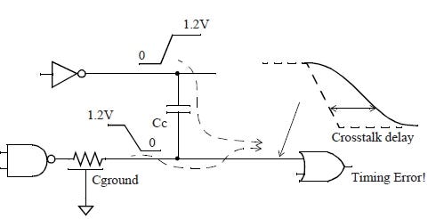
Crosstalk is a phenomenon by which a logic transmitted in vlsi circuit or a netwire creates undesired effect on the neighboring circuit or netswires due to capacitive coupling. Near-end-crosstalk Far-end-crosstalk 15. The tool calculates max.
And crosstalk in VLSIs IEEE Trans. The second part of this monograph presents techniques to model and alleviate off-chip inductive crosstalk. 12 DECEMBER 1999 1817 Short Papers Crosstalk in VLSI Interconnections Ashok Vittal Lauren Hui Chen Malgorzata Marek-Sadowska Kai-Ping Wang and Sherry Yang Abstract We address the problem of crosstalk computation and.
Not obscure the physical. 14 Crosstalk induced noise. During the transition on adjacent signal aggressor net causes a noise bumpglitch on constant signal victim net.
CRPR and Crosstalk Analysis. Crosstalk occurs via two mechanisms. For simplicity and for measuring the magnitude of noise induced on to the adjacent transmission lines we have to consider the two terms.
Crosstalk is a phenomenon by which a logic transmitted in vlsi circuit or a netwire creates undesired effect on the neighbouring circuit or netswires due to capacitive coupling. Signal integrity and crosstalk are quality checks of the clock routes. Refer to the digram below to get a clear picture on the effect of coupling capacitance on functionality and timing of VLSI circuits.
Time associated with the design of a new package is often not suited for the majority of VLSI designs. This is known as crosstalk. Crosstalk in VLSI interconnections.
Physical design levels and finally ways to face these challenges early in a. Crosstalk is the undesirable electrical interaction between two or more adjacent nets due to capacitive cross-coupling. What are VIAs in VLSI.
In the next section we would discuss the crosstalk mechanism in VLSI Design. Due to the influence of cross coupling capacitance switching of the signal from one net aggressor to the neighboring net victim. This video will give you a quick overview of various fixing methods that can be applied during eco implementation phase in ASIC physical design in VLSIFollo.
To connect between different metal layers we need poly layer along with the metal layers that we are going to connect. Therefore the second class of crosstalk noise modeling methods aims to further improve the efficiency of noise analysis such that they can be used in the inner loop of physical design. This work presents techniques to model and improve performance the performance ofVLSI designs without moving toward.
Physical design interview questionsphysical design interview questions in vlsivlsi physical design interview questionsphysical design interview questions vlsi4fresherscadence interview questionsphysical design interview questions pdf. Crosstalk induced noise Voltage profile of coupled noise Near end crosstalk is always positive currents from Lm and Cm always add and flow into the node. These values are defined so that optimization and analysis can ensure that the spurious signals.
When you perform crosstalk analysis using PrimeTime SI a change in delay due to crosstalk along the common segment of a clock path can be pessimistic but only for a zero-cycle check. From the below picture we can see that. Lets consider a buffer that is placed in a common path both data path and clock path for buf2 and buf3 buffer.
IEEE TRANSACTIONS ON COMPUTER-AIDED DESIGN OF INTEGRATED CIRCUITS AND SYSTEMS VOL. VIAs in VLSI. Crosstalk is the unwanted coupling of energy between two or more adjacent lines which can change the required signal and is also termed as Xtalk Occurs on long adjacent wires Can be interpreted as the coupling of energy from 1 line to another via.
Delays for setup calculation and min. Refer to the diagram below to get a clear picture on the effect of coupling capacitance on functionality and timing of VLSI circuits. Delays for hold worst- and best-case analysis.
However in deep submicron VLSI chip designs there is often the need to assess and avoid crosstalk noise in the early stages of the chip design flow.

Cts Part Ii Crosstalk And Useful Skew Vlsi Physical Design For Freshers

Team Vlsi Crosstalk Noise And Crosstalk Delay Effects Of Crosstalk

Mantra Vlsi Crosstalk Questions

Crosstalk Analysis And Its Impact On Timing In 7nm Technology By Einfochips An Arrow Company Medium

Team Vlsi Crosstalk Noise And Crosstalk Delay Effects Of Crosstalk

Optimization Of Crosstalk Delta Delay On Clock Nets
1 L24 Crosstalk Concerned Physical Design Jun Dong Cho Sungkyunkwan Univ Dept Ece Homepage Vada Skku Ac Kr Ppt Download

Cts Part Ii Crosstalk And Useful Skew Vlsi Physical Design For Freshers
0 comments
Post a Comment